Table of Contents
TogglePrinted Wiring Boards are crucial components of electronic devices that allow improved mechanical strength and electrical conductivity. To clear the confusion between PWB and PCB, we have created this blog to dive into the basics of PWBs, talking about their function, materials used, structure, and applications where these boards are used. By reading, you will better understand PWB and know the difference between PWBs and PCBs.
What is a Printed Wiring Board (PWB)?
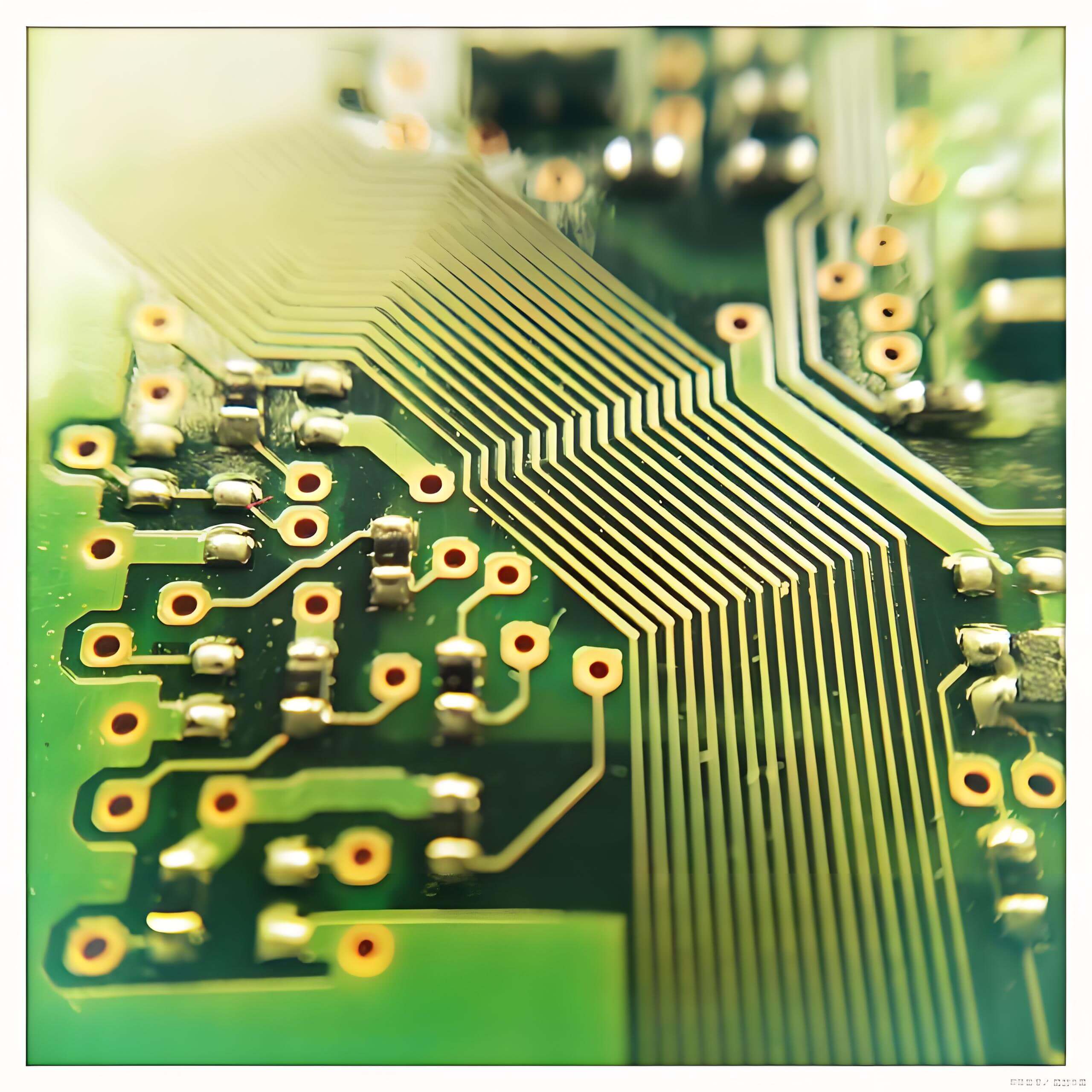
A Printed Wiring Board (PWB), on the other hand, is an older term that specifically refers to the board itself without any components attached. In other words, a PWB is a bare board that contains only the conductive pathways (wiring) and connection points for components. It was more commonly used in the early days of electronics.
Key Differences between PWBs and PCBs
People are often confused about PWB and PCB because the two terms are often used interchangeably today. Of course, this is also partly due to regional differences. Over time, the industry has basically used PCB as a standard term, whether it is an assembled board or a bare board. Therefore, in most cases, PCB is a globally recognized standard. Regarding the differences between PCB and PWB, we have already introduced what PWB is. Next, let's first understand what PCB is and then further explain the subtle differences between the two.
What is a Printed Circuit Board (PCB)?
A Printed Circuit Board (PCB) is the more commonly used term in the electronics industry. It refers to a board that mechanically supports and electrically connects electronic components using conductive tracks, pads, and other features etched from copper sheets laminated onto a non-conductive substrate (usually fiberglass or composite epoxy).
PCB vs. PWB
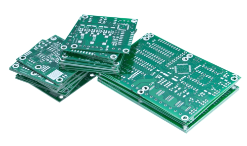
PCB is a circuit board that uses assembly technology (SMT or THT) to directly fix electrical connection parts on an insulating substrate, while PWB achieves conductivity by covering the surface of an insulating substrate with a layer of copper foil, and then uses chemical etching, drilling, and other processes to form circuit connections.
-
Scope of the Term
-
- PCB: Refers to the entire board, including the wiring and the components mounted on it.
- PWB: Refers only to the board with the conductive traces, excluding any components.
-
Usage Over Time
-
- PCB: The more modern and widely accepted term globally.
- PWB: An older term that is less commonly used today but may still appear in certain industries or regions.
-
Focus
-
- PCB: Emphasizes both the electrical and mechanical functions of the board.
- PWB: Focuses solely on the wiring aspect of the board.
In simple words. PWBs are the older version of PCBs. Although PWB and PCB have similarities and the two terms are sometimes used interchangeably in the PCB industry, there are still some differences between them. To present a clear view, here are the key differences between PWBs and PCBs:
|
Printed Wiring Board (PWB) |
Printed Circuit Board (PCB) |
|
|---|---|---|
|
Structure |
Printed directly onto the fiberglass |
Several layers of components, connectors, and traces are all bundled together |
|
Performance |
More speed, reliability, and the ability to carry frequencies |
Limited when talking about propagating higher frequencies |
|
Process |
Conductive traces that are directly printed on the fiberboard |
Go through an extensive process that includes steps such as drilling, laminating, etching, and insulating the layers/components |
|
Cost |
Lower |
Higher |
|
Region |
Japan |
United State |
Components in PWB Assembly
A variety of materials and components are involved in the assembly of PWBs. Altogether, these components pile up together to create a circuit that can perform functions as defined by the requirements. The components involve the following.
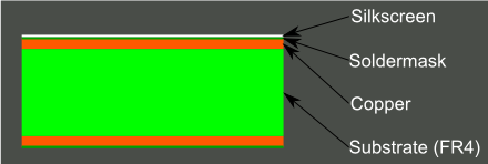
- Base material: Also known as substrate, it is the base material that helps in providing the physical structure of the board. It is made from materials like fiber and acrylic.
- Copper traces: The PWB boards contain copper traces that are created using the print technology and then dipping the board in acid. These traces help in carrying the signals and provide connections between a series of components.
- Solder mask: Layers of solder masks are present on all PWB boards to guard against short circuits and component damage.
- Silkscreen: Silkscreen is the term used to describe the writing, component names, and logos on PWB boards. PWBs contain silkscreen so that users can identify where to place components.
Step-by-Step PWB Manufacturing Process
PWBs follow a detailed manufacturing process that allows these boards to function properly. To create a PWB board, here are the Step-by-Step Manufacturing Processes of PWBs that are involved.
- Step 1: Layout Design
The first step that is involved in manufacturing Printed Wiring Boards is creating the design layout. This is done through the help of schematic design using software such as Altium and KiCad.
- Step 2: Materials Preparation
After the schematics and design are done, the materials are selected for the substrate. This depends on the application of the board and where it is going to be used. The materials can be fiber, flexible, or metal core.
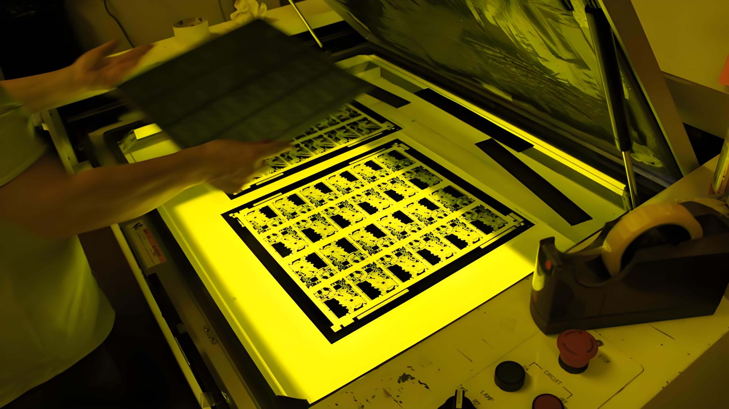
- Step 3: Copper Cladding & Etching
In order to create the traces, a thin layer of copper is applied to the substrate. Then, the circuit is printed on the plate and excess copper is removed through the etching process.
- Step 4: Drilling / Plating
Once, the board is passed through the etching process, the drills are holed and used for connecting components using leads and vias.
- Step 5: Solder Mask Application
The solder mask layer is applied after the above process. The mask prevents components from getting shorted. It also protects the traces on the board.
- Step 6: Component Assembly
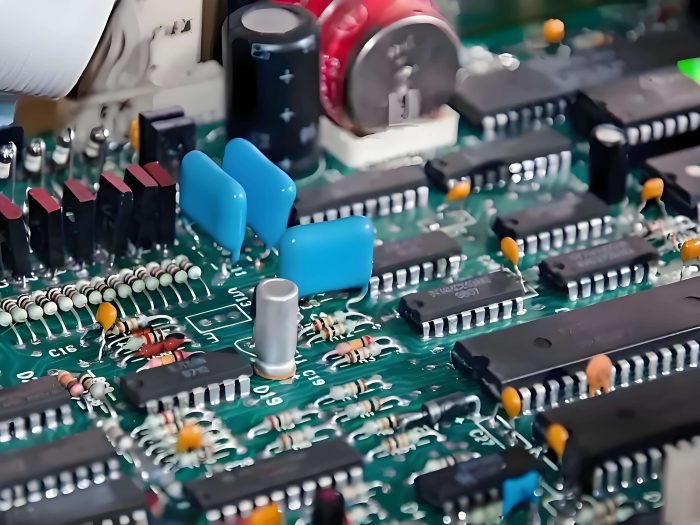
The PWB manufacturing process involves the process of adding and mounting components such as SMT and SMD. These components are mounted directly and are soldered using machines.
- Step 7: Testing & Quality Control
After every step is followed, the printed wiring boards are passed through an extensive quality control process to ensure that the boards are up to standard.
Terminology Related to PWB
- PCB (Printed Circuit Board): A flat board that electrically connects and supports electronic components using conductive pathways etched from copper sheets.
- PCBA (Printed Circuit Board Assembly): The complete assembly of a PCB with all electronic components soldered onto it, ready for use in electronic devices.
- PWB (Printed Wiring Board): Similar to PCB, this term emphasizes the electrical connections made on the board rather than the components themselves.
- PWA (Printed Wiring Assembly): Refers to a PWB that has been populated with components but may not yet be fully assembled or soldered.
- CCA (Circuit Card Assembly): A broader term that includes any assembly of circuits, typically referring to the complete unit including the PCB and all mounted components.
If you want to learn the difference between PCB and PCBA, read the following blog:
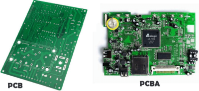
PCB vs PCBA: Key Differences in Circuit Board Manufacturing
Learn the critical differences between PCB and PCBA. Understand their roles in electronics manufacturing. Understand the benefits and trade-offs of using SMT, THT, and mixed technology. Understand why choosing the right manufacturing process is essential for high-quality electronic products.
Conclusion
Printed Wiring Boards (PWBs) are a crucial element in modern electronics and act as a strong backbone, allowing for improved connectivity for a variety of devices. From automotive ECUs to consumer electronics and industrial machines, PWBs play an important role in advancing technology, providing us with devices that we see in the market.
Even though PCB has gone mainstream, recognizing these key terms is a small step to success. Whether you're an engineer, an amateur, or a beginner who wants to learn more about the industry, feel free to contact us if you have any more ideas.