Table of Contents
ToggleIn the production of printed circuit boards (PCBs), a solder mask is an important component that is frequently overlooked but is necessary to guarantee the functionality and reliability of electronic devices. Applied to the PCB surface, this protective layer has several uses beyond simply giving the board its distinctive green color. This blog post will discuss soldermask type, color, thickness, apply process, defects, and how they improve the general functionality and longevity of electronic components.
What is a Solder Mask Or Solder Resist?
Solder mask also known as solder resist and solder top. To limit solder spreading and avoid solder bridges during assembly, PCBs are coated with an older mask, which is a protective polymer coating. Additionally, it assists in shielding traces from electrical leakage and environmental deterioration. It serves in diverse ways like:
- Preventing environmental corrosion and oxidation of exposed copper
- Avoiding the formation of solder bridges during assembly between closely spaced pads
- Live nets that are electrically insulated to avoid shorting
- Permitting selective coating or plating of exposed portions
Why Use Solder Mask on PCB Boards?
In the production of PCBs, soldering mask is a crucial protective coating. Using solder resist has the following main advantages:
● Insulation:
The solder mask layer improves electrical reliability by insulating the board and preventing shorts between closely spaced traces or pads.
● Solderability:
Copper traces and pads are made more solderable by solder resist, which stops oxidation. It guarantees strong and dependable connections.
To facilitate automated assembly, the soldermask delineates pads and regions for component placement.
● Contamination Protection:
The coating prolongs the board's usable life by guarding against corrosion and environmental contaminants.
● Aesthetics:
To visually identify solder and non-solder portions for quality monitoring, many solder masks are green or another color.
What are the Types of PCB Solder Mask?
1. Epoxy Liquid
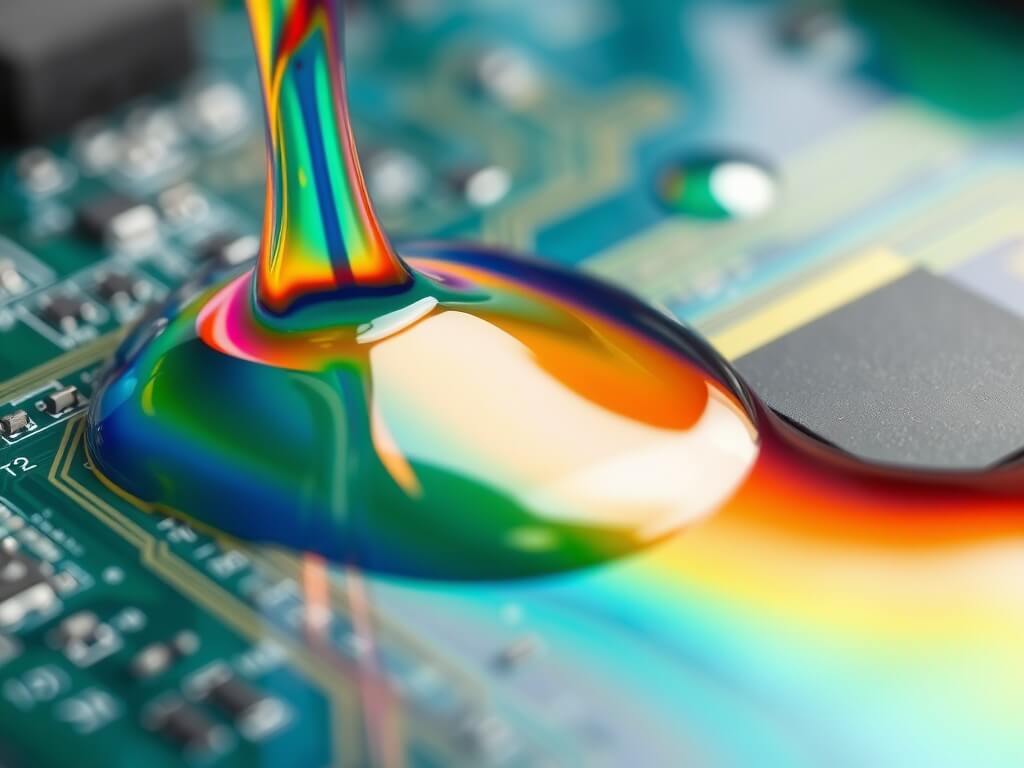
Epoxy liquid is one type of photosensitive liquid polymer that is commonly used as a solder mask layer. It is composed of a solvent-dissolved photo-initiator and epoxy resin. When exposed to UV light through a photomask, the photo-initiator triggers a chemical process that solidifies and crosslinks the exposed epoxy resin.
The circuit board solder mask can subsequently be formed by washing away the unexposed areas of the cured patterned epoxy coating. This process gives the epoxy liquid PCB solder mask exceptional adhesion and thermal, and chemical resistance. It is widely used in PCB manufacturing due to its excellent insulating properties. It has several benefits like:
- The most popular and economical type
- UV light exposure cures
- Available in various colors, like green, blue, and red.
2. Dry Film Solder Mask or DFSM
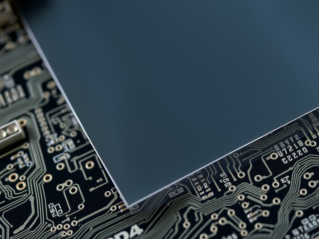
It is a circuit board mask layer made of photosensitive laminate. It is made up of polymer films encased in photosensitive epoxy or polyimide resin. The procedure entails using pressure and heat to laminate the dry film onto the copper-clad board. The resin layer is bonded to the board in this way. The resin is then hardened in the specified pattern by exposing it to UV light using a photomask. The cured soldermask pattern is left behind after development eliminating the unexposed portions.
This indicates that no solvents are needed for application or development. Similar to liquid resins, it has high insulating qualities and board adherence. Its benefits include:
- The technique is solventless and the thin film thickness is uniform.
- Its handling and registration are simple.
- And the insulation and adhesion are good.
3. Liquid Photo-imageable Solder Mask or LPSM/LPI
A liquid photo-imageable (LPI) polymer substance is used as the PCB solder mask layer in LPSM (Liquid Photo-imageable Solder Mask). The LPI is made of a photo-acid generator combined with a liquid resin based on epoxy. The photo-acid generator creates acid to catalyze the resin's crosslinking reaction when it is exposed to UV light through a photomask.
The cured patterned LPI solder mask layer can then be removed by developing the unexposed portions. PCBs with fine geometries and features can be consistently coated with LPI solder masks owing to this light-sensitive, liquid-based working technique. Its benefits include:
- Allows for high-resolution imaging and intricate patterns & design
- Offer a consistent coating thickness across the PCB surface
- Excellent resistance to chemicals and environmental factors

4. Silicone-Based & Urethane Acrylate Solder Masks
It can withstand extreme heat and be adaptable. Also, it is used on high-temperature or flexible boards and is more expensive than epoxy.
5. Epoxy Powder Coating
It is applied as a dry powder and allowed to cure and less expensive yet less competent primarily restricted to consumer goods.
6. Flame Retardant Solder Masks
Fulfill flammability requirements to ensure safety compliance and frequently apply to consumer products.
How to Apply Solder Mask on PCB?
On PCBs, the circuit board solder mask is a basic defensive layer that watches against oxidation, natural harm, and inadvertent patch bridges. A few correct strategies are included within the application to ensure functionality and quality:
Step1: Cleaning the PCB Surface
Sometimes after applying the solder, the PCB surface must be altogether cleaned to expel any contaminants, tidy, and oxidate. To guarantee that the mask follows accurately, this step is required. Cleaning as often as possible involves:
- Chemical cleaning: To get rid of residues and oils.
- Mechanical scrubbing: The copper surface is prepared by mechanical scrubbing.
Step2: Applying the PCB Solder Mask Layer
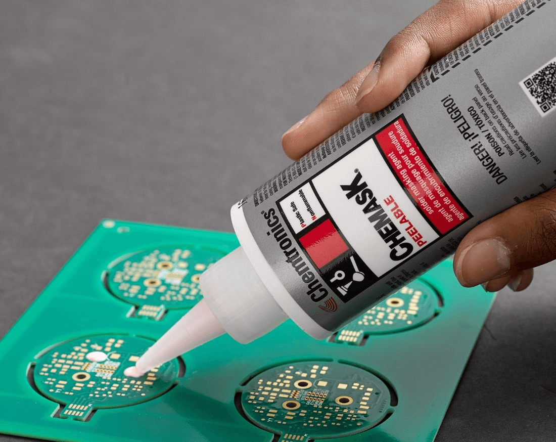
After the board has been cleaned, the solder resist material, typically a fluid photo-imageable (LPI) epoxy or ink, is applied. It can be connected in three common ways:
- Screen Printing, which employs a stencil to store the PCB solder resist onto particular PCB zones;
- Curtain Coating, which covers the PCB evenly by having it pass through a curtain of liquid solder resist material;
- Shower Coating, which guarantees reliable application on complex or uneven PCB surfaces.
Step3: Pre-Drying
The board goes through a pre-drying method to somewhat harden the soldermask once it has been connected. Delicate heating may be a handle that makes a difference: the PCB solder mask adheres to the PCB and gets it prepared for the after-step.
Step4: UV Exposure While Masking
A photomask, which could be a clear film with the circuit board solder mask design on it, is put over the PCB. The board is at that point uncovered to ultraviolet light. The UV-exposed regions solidify, whereas the unexposed areas stay delicate and can be evacuated afterward. This step guarantees that, as suitable PCB regions receive solder resist.
Step5: Developing
The PCB is passed through a developer solution to expel the unhardened solder mask material. This step appears in the copper pads and gaps that will afterward be utilized to solder components.
Step6: Last Curing
The PCB is either subjected to UV light or cured in an oven to fully solidify the soldering mask. This last curing step guarantees strength and resistance to warmth, chemicals, and physical wear.
What Color Should a Solder Mask Be?
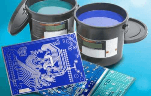
The color of your solder resist comes from the dye in the material, and the type of dye can change how thick the finished solder mask is. Green solder masks are popular because they can create very thin barriers (about 0. 1 mm). Other colors of dye usually make thicker barriers.
There are rules ( IPCSM840D) that explain how thick the soldermask should be for different industries or uses. Black solder masks can make it hard to see the board and wires, which can be a problem for automated checks. Also, the color of your silkscreen can affect how easy it is to see details and can cause eye strain during manual checks.
What is the Standard Solder Mask Thickness?
IPCSM840D says there is a limit on how thick the PCB solder mask can be, but it doesn't specify exact thicknesses like 20 or 25 micrometers. The company that makes the circuit boards is responsible for making sure that the board has minimum solder mask thickness. To check this thickness, they can use a micrometer that is accurate to 25 micrometers or a specific testing method.
If a certain thickness or breakdown voltage is needed, it should be agreed upon by both the supplier and the user. When tested using a certain method, the circuit board solder mask material must have a breakdown voltage of at least 500 VDC for every 25 micrometers of thickness. If the solder mask is thinner than 25 micrometers, it must still have a minimum breakdown voltage of 500 VDC.
Solder Mask vs. Solder Paste
The following table shows the difference between solder mask and solder paste, which may help you better understand their difference in various aspects.
|
Specifications |
Solder Mask |
Solder Paste |
|---|---|---|
|
Definition |
protective layer to shield areas from soldering |
powdered solder alloy to bond components to the PCB |
|
Material |
Polymer-based material |
Metal solder powder (tin, lead, or lead-free alloy) and flux |
|
Purpose |
Protects the PCB surface |
Temporarily adheres and electrically connects components |
|
Application |
During PCB manufacturing |
During PCB Assembly |
|
Physical State |
Solid, cured coating |
Paste-like, semi-liquid substance |
|
Key Function |
Acts as an insulator and prevents solder bridges |
Forms solder joints between components and PCB pads |
|
Color |
Green, blue, red, black, or other colors |
Silver-gray, paste-like |
|
Removal |
Permanent once applied and cured |
Evaporates during reflow, leaving only solder behind |
Common Solder Mask Defects & Causes
Solder masking can have problems that might impact quality and reliability, just like other manufacturing processes. Here are some of the most common mistakes:
- Solder bridging:
- Defect: Solder bridging happens when the solder connects two close contacts or pads, which can cause an electrical problem.
- Cause: It often happens because too much solder paste is used, leftover flux stays on the board, or the board isn’t cleaned well after soldering.
- Pinholes:
- Defect: These tiny holes in the circuit board solder mask layer show the copper underneath. Shorts can happen if there are tiny holes that let solder go under the parts during the heating process.
- Cause: They might be caused by not curing properly or by contamination when putting on the soldering mask.
- Peeling/Delamination:
- Defect: Peeling or delamination happens when the circuit board solder mask layer comes apart from the board. Copper that gets exposed from peeling can break down over time, which may cause weak connections in soldering or other electrical issues.
- Cause: This usually happens when the solder mask and the board materials don't work well together, or if the board isn't ready before putting on the PCB solder mask.
- Absent Soldering Mask:
- Defect: You can see copper when there is no mask at all. During reflow, it helps the solder attach to the open copper areas.
- Cause: This is often because of mistakes in using the application, like blocked stencils.
Conclusion
The green coating on the soldering mask might seem like it's just for looks, but it actually serves several important functions for making strong and reliable printed circuit boards. Special solder masks that are designed for specific uses can improve the success rates of putting together PCBs, strengthen solder connections, and make them last longer if they are made, selected, and used correctly. Working closely with your board manufacturing partners ensures that the solder mask is customized to fit your products according to their capabilities and expertise.
Frequently Asked Questions
How to remove solder mask?
Although solder mask is generally considered permanent once applied and cured on a PCB, it can be removed in several ways:
- Mechanical Removal: scrape with an X-Acto knife or fine files
- Chemical Removal: apply a solder mask remover, allowing it to sit, then use a soft brush to wipe it away, followed by rinsing with isopropyl alcohol.
- Laser Removal: vaporizing the soldering mask without harming the board in professional settings.
What is a paste layer in PCB?
On surface-mount pads, the paste layer marks areas for putting solder paste, ensuring that components are placed correctly and that connections are reliable during assembly.
What causes solder mask scratches, nicks, or tears?
Bad handling, rough production methods, faulty materials, not curing properly, or bumps during assembly can all lead to damage to the PCB solder mask.
When is a solder mask touch-up or reapplication needed?
Touch-up is needed after fixing a PCB when scratches show copper lines or when we find problems like peeling paint or uneven surfaces during inspection.
What are some key considerations when selecting a solder mask type?
When picking a circuit board solder mask, consider how you will apply it, the color you like, how much it costs, how well it can resist environmental conditions, and whether it works well with the materials and methods of the PCB.