Blog

With the rapid development of science and technology, the packaging requirements for integrated circuits are now more stringent. Nowadays, to meet development, the ball grid array package has also appeared. BGA is a novel technology in SMT assembly. It is a popular way to assemble chips on PCB boards and has won wide attention in the PCB industry
 
As China’s most trustworthy supplier, FC PCBA’s BGA assembly services are specifically tailored to today’s electronics, ensuring that our customers’ requirements for BGA integration in their PCB designs are met with precision and quality.

What is Ball Grid Array (BGA)?

Before BGA, techniques such as dual in-line packages (DIP) and flat packages were used in the PCB assembly. The research identified the issues in the pin grid array integrated circuits that the larger number of pins in less space compromises the reliability and performance of complex applications. To solve these problems, BGA was developed.

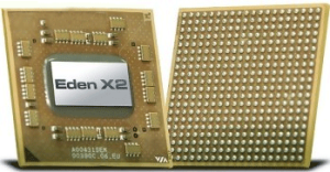
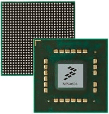
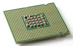
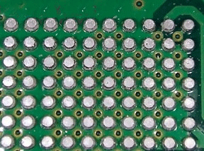
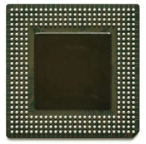
BGA is a technique to mount complex chips or integrated circuits such as microcontrollers or microprocessors on PCB Boards. BGA introduced a minimal solder ball array on the bottom of chips. In BGA, these chips have some solder balls on the bottom. The chips are connected to the PCB by these solder balls, which makes the connection more reliable and saves the space of the PCB. Using BGA, a larger number of pins can be designed in a chip in the shape of solder balls in less space, and more than that, the distance between the chip and PCB is lesser.

ball grid array (bga)

 Therefore, BGA packaging technology is dominant in the electronics manufacturing industry nowadays.

Types of BGA Packages

Depending on the performance requirements and the type of application, FC has evolved to produce the following ball grid array package types:

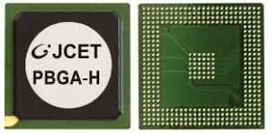
Plastic Ball Grid Array (PBGA)

Plastic Ball Grid Array (PBGA) is the most common BGA packaging, with a plastic substrate that provides a light-weight integrated circuit solution. Solder balls are mounted on the bottom side of the package to allow high-density interconnections (HDI). PBGA is used in consumer electronics, telecommunications, and computing due to good thermal performance, ease of manufacturing, and surface-mount technology (SMT) compatibility. Its thermal and mechanical performance, however, is usually lower than that of ceramic-based BGAs, and thus it is less suitable for high-reliability applications.

Ceramic Ball Grid Array (CBGA)

Ceramic Ball Grid Array (CBGA) is a ceramic substrate-based BGA with higher thermal conductivity, mechanical strength, and reliability compared to plastic BGAs. The ceramic substrate possesses excellent heat dissipation, so CBGA finds a good fit in high-power and high-frequency applications such as telecommunication, aerospace, military, automotive, and high-end computing. CBGA packages weigh more and are more expensive than PBGAs, however, so their use is limited in cost-sensitive or weight-critical applications. The rigidity of CBGA also makes it less forgiving of mechanical stress, requiring careful handling during assembly.

Ceramic Ball Grid Array (CBGA)

Flip Chip Ball Grid Array (FCBGA)

Flip Chip Ball Grid Array (FCBGA) is a combination of flip-chip technology in a BGA package where the semiconductor die is flipped and soldered upside-down directly onto the substrate with solder bumps. FCBGA is commonly used in high-performance devices like CPUs, GPUs, and network chips. The package offers excellent signal integrity and power delivery but requires very precise manufacturing processes and is hence more complex and costly than traditional wire-bonded BGAs.

Tape Ball Grid Array (TBGA)

Tape Ball Grid Array (TBGA) employs a flexible polyimide tape as the substrate instead of rigid plastic or ceramic. Weight saving and a thinner package profile make TBGA suitable for space-constrained and portable devices like smartphones and tablets. The tape substrate also provides flexibility, improving mechanical stress resistance. TBGA is less thermally conductive than CBGA or FCBGA, limiting TBGA’s use in high-power devices.

Tape Ball Grid Array (TBGA)

Enhanced Ball Grid Array (EBGA)

Enhanced Ball Grid Array(EBGA) is a thermal EBGA IC package method that has better thermal and electrical performance through new materials and design enhancements. It may employ heat spreaders, thermal vias, or high-conductivity substrates for enhanced heat spreading. EBGA is typically applied in applications requiring increased reliability and thermal management than standard PBGA, such as automotive electronics and industrial systems.

Enhanced Ball Grid Array (EBGA)

Metal Ball Grid Array (MBGA)

Metal Ball Grid Array (MBGA) employs a metal substrate, like copper or aluminum, to provide improved thermal and mechanical performance. MBGA’s metal base functions as a good heat spreader, making MBGA appropriate for power-intensive and temperature-intensive applications like power electronics and LED modules. MBGA is heavier and more expensive than plastic or tape-based BGAs and therefore is limited to specialty applications where thermal performance is critical.

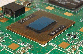
Micro Ball Grid Array (μBGA)

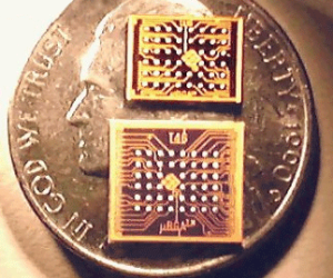
Microball Grid Array (μBGA) is a smaller BGA. It is constructed on packaging tape, with the die facing down always. An elastomer between the tape and die helps in the removal of thermal expansion stress. It is the foundation of low pin count high memory products, developed for ultra-compact and high-density applications such as mobiles, wearables, and medical implants. The package has extremely fine solder balls and pitch, allowing for more interconnects in a smaller area. μBGA has good electrical performance due to low parasitics, but requires advanced manufacturing and assembly technologies.

Micro Ball Grid Array (μBGA)

The BGA Assembly Process at FC

We already know that the BGA package has the advantages of high density, high reliability, and good electrical performance, which is widely used in electronic products. Next, we will introduce the BGA assembly process at FC in detail.

Step1: Initial Design and Layout

The design of a BGA package is a task of precision. There is no chance of any mild error. Even a small deviation can fail in the entire process. To design successfully, one should plan each step initially, from component placement to the layout of pathways.

Step2: Solder Paste Application

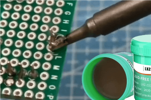
One of the most challenging parts of the BGA assembly process is to solder paste. Usually use lead-free solder paste for coating. Spread the lead-free solder paste evenly on the substrate to ensure that the thickness of the coating layer is uniform and not too thick. Use a scraper or other tools to scrape the lead-free solder tone to ensure the flatness of the coating layer. There are multiple techniques to gain consistency in the entire process. Viscosity control and stencil calibration must be performed to obtain better results.

Step3: Ball Array Arrangement

Ball Array Arrangement is the third step of BGA assembly, mainly arranging the solder balls at specific positions on the substrate.
 
  • Solder Ball Selection
The selection of solder balls is based on factors such as the number and size of chip pins. Solder balls are generally made of lead-free alloys with good soldering performance and reliability.
 
  • Soldier Ball Arrangement
The solder ball arrangement is to paste the solder ball in a specific position on the substrate, corresponding to the chip pins. Place the solder balls in the specific positions to maintain alignment accuracy. Use a hot air gun or hot plate to heat the melted solder balls and bond them with the lead-free solder paste on the substrate.
PCB component placement

Step4: Solder Ball Connection

Solder ball connection is the core step of BGA assembly, mainly connecting the chip to the solder balls on the substrate. It is placing the chip on the substrate to maintain alignment accuracy. The solder balls are heated using soldering equipment to melt them. The soldering temperature and time are controlled to ensure the quality of the connection between the solder balls and the chip pins.

Step5:Cleaning

Cleaning is to remove the solder slag and dirt produced during the soldering process to ensure product reliability. Specific steps are as follows, the packaged chip into the cleaning solution for ultrasonic cleaning. -Remove the chip and rinse it with deionized water to remove the residue of the cleaning solution.
Reflow soldering

Step6:Inspection and Testing

After the process of BGA assembly, inspecting and testing the assembled PCB is also an important method. A single wrong soldering on the PCB board can result in a short circuit in the control board when powered. Therefore, some testing and inspection techniques are required to maintain the quality of the assembly. The testing method checks each detail of the PCB to verify the assembled PCB.

Advantages of BGA Assembly

Performance Enhancement

BGA assembly provides an enhancement in electrical performance by reducing the distance between the PCB and the chip. It makes efficient and fast signal communication.

Space Efficiency

The compact design of BGA packages saves valuable space on the PCB, it allows for numerous components in less area of the PCB.
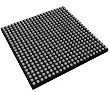
ball grid array (bga)

Enhanced Reliability

The solder ball connections in BGA assemblies provide strong and reliable physical connections. It ensures reliability and performance.

Heat Dissipation

Various types of BGA packages offer excellent thermal performance. In complex devices, BGA technology dominates in reducing the risk of overheating.

Challenges in BGA Assembly

Soldering Issues

BGA package integrated circuits is a compact package composed of small soldering balls, which is a challenge to program for soldering with precision and a small mistake can ruin the PCB board.

Inspection Difficulties

Inspecting the assembly process is a useful procedure to check the quality of the assembly. However, Inspection requires advanced techniques and attention to ensure that every connection is perfectly established and non-errors.

Rework and Repair Challenges

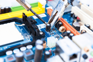
When a PCB becomes faulty and comes for repair, the BGA ICs are very difficult to resell, and a new IC on the same pad with the same accuracy without damaging any traces. It’s a complex task to perform manually or automated. It involves various techniques to repair the PCB.

Comparison with Other Packaging Technologies

BGA vs. QFP

BGA and QFP differ mainly in design and application. BGA uses solder balls, which provide better performance and reliability, while QFP relies on fine pins that can be more delicate and harder to handle.

BGA vs. CSP

When comparing BGA to CSP, BGA often wins in its performance, while CSP is slightly better in space efficiency due to its smaller size. Both are great, but the choice depends on specific needs.

BGA vs. LGA

BGA provides a strong solder connection, while LGA uses flat contacts. This makes BGAs easier to replace or upgrade components. Each has its benefits, with BGA being more robust and LGA being more flexible.

Applications of BGA Technology

Consumer Electronics

BGA technology is common in smartphones, smartwatches, laptops, and many other devices. It helps improve their performance and reliability.

Telecommunications Industry

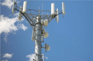
BGA is essential in networking equipment. It ensures efficient data transmission and receiving and strong connectivity.

Automotive Industry

In vehicles, especially electric vehicles, where High-frequency servo drives, and BMS systems are used BGA is an important aspect of the automotive industry. It supports advanced features and safety systems.

Medical Devices

Nowadays, the medical industry has developed many portable healthcare devices that are small but require greater accuracy. They also use BGA technology. It provides precision and durability in important healthcare tools
Ball Grid array is an advanced technology designed to improve performance, reliability, and thermal quality. It is an excellent technique to save space on PCB. BGA assembly is useful for high-speed, complex devices, It is an innovative achievement in consumer electronics, automotive, telecommunications, and healthcare industries. Despite challenges like precise soldering and detailed inspections, various advantages include enhanced electrical performance, strong connections, reliability, and better heat management. As technology advances, BGA assembly will continue to play a crucial role in developing more advanced and reliable electronic devices.
 

FAQs

Common issues include soldering defects, inspection challenges, and difficulties in reworking or repairing BGA components.
BGA stands for Ball Grid Array is a technology used to mount integrated circuits on PCB boards.
 
BGA is preferred for its enhanced performance, reliability, and space efficiency, making it ideal for high-speed and complex electronic devices.
BGA components are difficult to reuse due to the complexity of resoldering and replacing them without damaging the PCB.
BGA assembly is inspected using various techniques such as automated optical inspections and electrical testing to ensure quality and reliability.
Shop
Wishlist
0 items Cart
My account